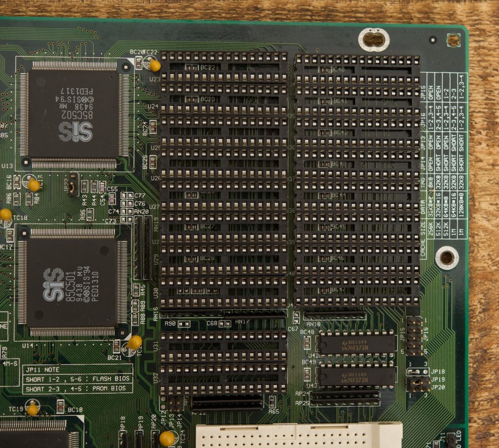
I’ve just got my hands on this beautiful Socket 4 motherboard – the ELITEGROUP (ECS) model SI5PI. The motherboard is using SiS 501 series chipset. It has one really unique feature – 16 DIP sockets for L2 cache + 2 extra sockets for cache tag chips.
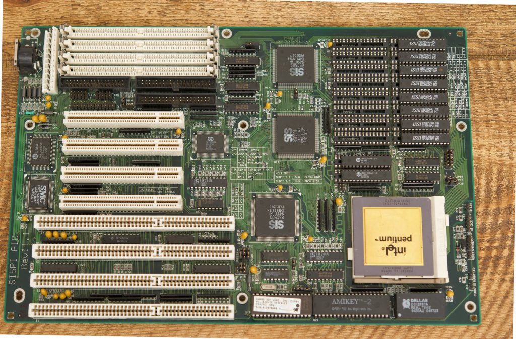
Furthermore, all these sockets are DIP32 sockets. That means they can accommodate 1024 kbit chips giving you not less than 2048kB of L2 cache. Something that was unheard of in 1994 when this motherboard was new and wasn’t common until much later. In that period boards typically had like 256kB of L2 cache (if any at all). The high-end workstation or server boards sometimes came with 512kB.
It is a well-known fact that the performance improvement is not proportional to the cache size increase. You get the most bang by having at least some cache. Each doubling gives you just a tiny bit of extra performance.
However, in retro computing, we don’t operate on the value/cost principle. Empty sockets are just an invitation to fill them with chips and maximise the performance. However, in order to do that I had to solve 2 problems first:
- Getting the 1024kBit SRAM chips
- Configuring the motherboard to recognise them
The first task wasn’t as easy as it seems. Yes, there are Asian sellers on eBay and other places you can buy DIP32 SRAM chips from. They are relatively cheap. But you get what you pay for.
I found listings with IS61C1024-10N marked chips. The -10N suffix looks suspicious already as, according to the ISSI datasheet, this particular chip wasn’t available in 10ns variant. That’s a warning sign as we are dealing with what’s likely a slower relabeled part. There are also IS61C1024-15N chips, but who knows if these are genuine.
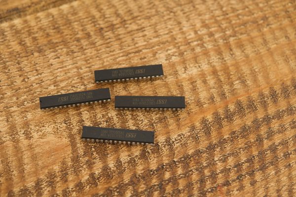
When I got the chips I noticed that like 30-40% of them are faulty, so I need to reorder a couple of times. Testing 18 SRAM chips for stability was a tedious task itself. Basically I was swapping the chips in my single-bank 486 board until the system was stable.
Eventually, I got 18 working chips. So I inserted them into the motherboard and started wondering about how to set configuration jumpers to get them recognised.
I have no manual and all online resources as well as the table printed on the board end up at 1024k (in either single or dual bank version):

So I took a multimeter and started to find out the wiring scheme to be roughly as follows:

There are two sets of jumpers. One of them, JP12/JP13/JP14, seems to be configuring the tag SRAM size as they wire high address bits of TAG chips to D58, D61 and D62 pins of the CPU (most likely via chipset).
The second group is 5-position JP15 and JP16. These jumpers create links of address bits between banks. This seems to inform the chipset how many data chips you have and how big they are.
Extrapolating the table of “normal” cache sizes I figured out the likely setting for 2M.
- JP12 – short
- JP13 – short
- JP14 – short
- JP15 – 2-4 and 4-5
- JP16 – 2-4 and 4-5
The only problem is that on my board the JP12 pin header is not present. So I had to solder it in.

I was hoping that, given the dual-bank setup, I should be able to run the board with maximum BIOS settings. However, for the sake of system stability it was necessary to reduce the cache settings by one step as follows:
That’s not too bad but still one step below the absolute maximum. Not sure if it is because of the board or the fake chips, but it also means this board still has some tuning potential.
With all chips present and those settings applied the board correctly boots and proudly shows 2048k size in the POST table:
The cachechk tool seems to correctly detect the cache size:

The speedsys shows a rather unusual graph:

OK. The cache works. OK. Mission accomplished!
Hello there!
Awesome work – a 2MB vintage Pentium board is quite The retro stunner, especially a high quality one like the SI5PI… the battleship of early 586-allure(besides the R512 and most likely some obscure server hardware).
Thanks again for providing me with a BIOS.
If you’re using CF disks – which ones are working for you?
Take care,
Viktor
Hi. Thanks!
as I am dealing with 486 or early Pentium era HW, the onboard IDE is often absent or unreliable (CMD640 corruption). Even PCI IDE cards don’t work without issues as the PCI IDE spec was finalised much later than PCI.
Thus I like to use Adaptec SCSI cards for PCI/ISA/VLB buses + SD2SCSI v6 device + SD card. That way I can bypass the BIOS and have consistent compatibility and performance.
Interesting,
I’ll keep that in mind. I often wondered about some boards showing seemingly random problems with hard drives / CF cards.
Take care
SCSI was vastly better anyways in that era since it didn’t interrupt the cpu. Even today’s SAS drives to a certain extent are also better than SATA in the same way–less CPU interruptions.
We used SCSI on both our 486 and P166+ builds back in the day. Still have both systems too, but they need restoration.