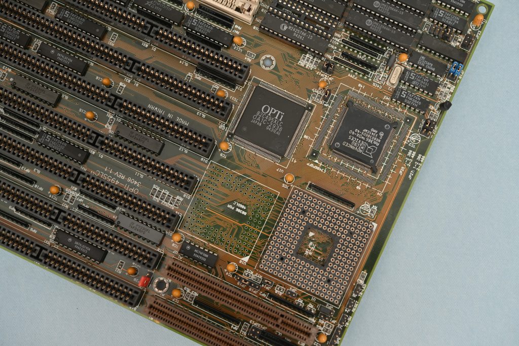
I was wondering what would be the ultimate upgrade for my 386 motherboard. It has a soldered-in 386 CPU, an unpopulated 386 PGA socket, and a socket for either a 387 FPU or a 486 PGA. It might even be compatible with a Weitek processor, though I’m not entirely certain. There’s also a possibility that it has a soldered-in 486SX PQFP. As you can see, there are plenty of options available.
But what if I attempted to install a Pentium CPU through some creative tinkering?
Of course, the initial challenge lies in the fact that my motherboard lacks the required Socket 2 for a Pentium Overdrive, not to mention the more advanced Socket 3. It doesn’t even feature a Socket 1. Instead, it boasts a hybrid socket designed to accommodate either a 486 PGA CPU or a 387 FPU (in the scenario where a 386DX CPU is already in place).
However, upon examining the Pentium Overdrive pinout, the additional row of pins doesn’t appear to be essential at all. It mainly consists of extra power points and some signaling pins to facilitate L1 cache coherency when utilizing write-back functionality. There’s nothing overly concerning here. Conveniently, the PODP (Pentium OverDrive Processor) doesn’t utilize the 486 write-back cache controls like the DX4 or 5×86 does. As a result, the WB/WT (Write-Back / Write-Through) pin remains unconnected, eliminating the need to reconfigure the board for P24T mode, as you would on a standard 486 motherboard.
I didn’t find it worthwhile to configure any jumpers and opted to leave the board set up for 486SX mode.”

As the socket wasn’t designed for much wider PODP it helps to use a PGA169 socket to lift the wide CPU up a bit so that the unused row of pins doesn’t interfere with jumpers and other components that are in surrounding of the CPU socket.
The resulting combo looks quite weird:
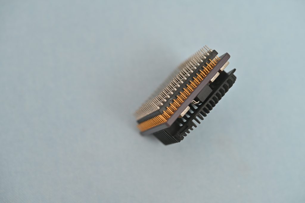
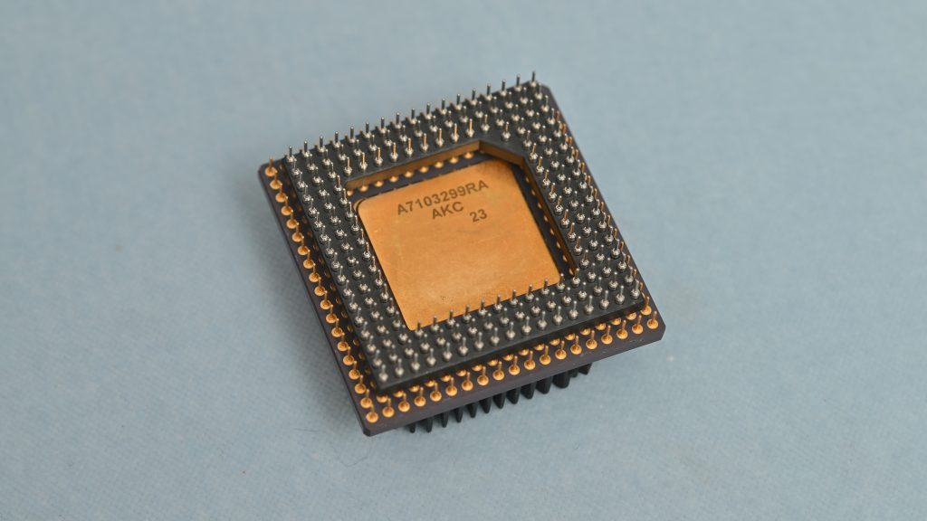
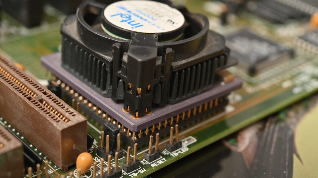
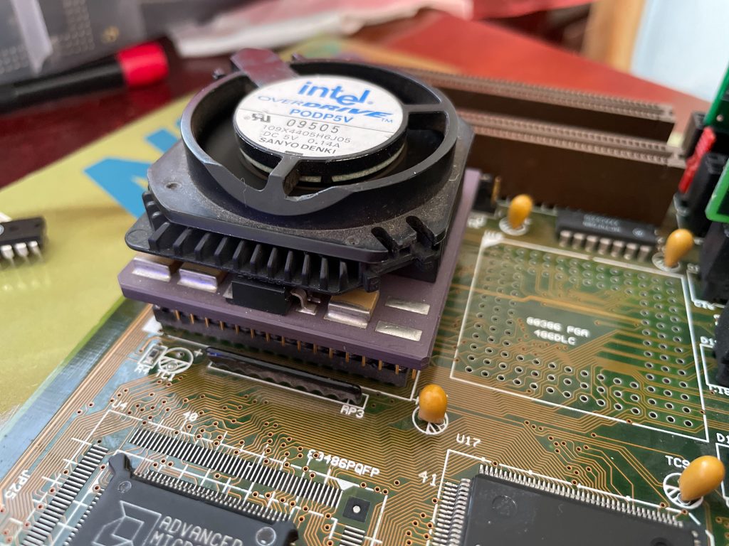
However, who cares about how it looks from bottom. It looks OK when installed.
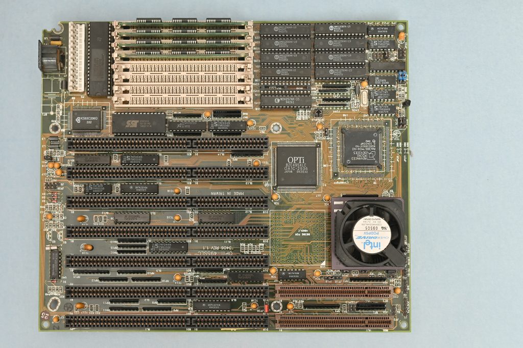
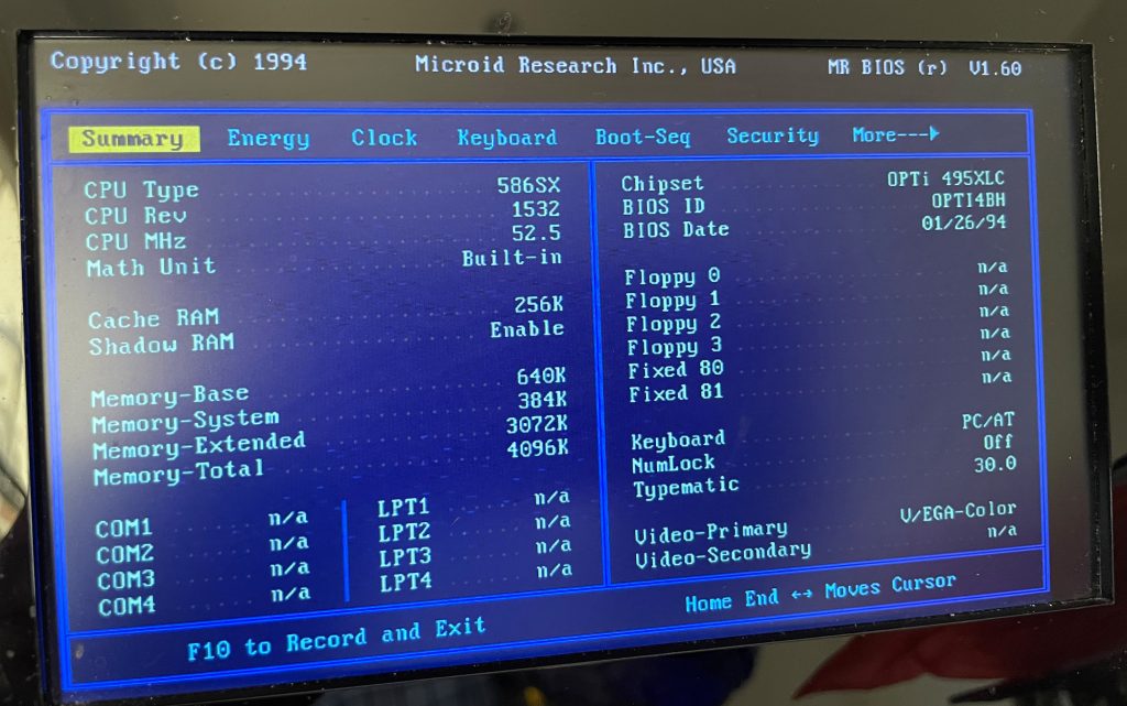
And believe it or not, it runs fine. The MR BIOS on my board is quite confused and reports the CPU to be 586SX, which I like.
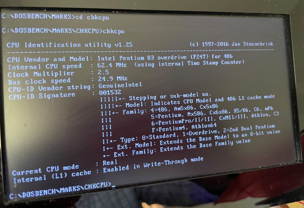
Obviously, the performance is slower than newer 486 boards, the L1 runs in write-through mode, but it runs just fine.
I thought there must be a reason for the PODP having the extra power pins. Just to play it safely I configured maximum power on my ATX2AT device and set the frequency to 25MHz. However, it turns out that idling only @ 3.6A – not too far from ordinary 486DX.
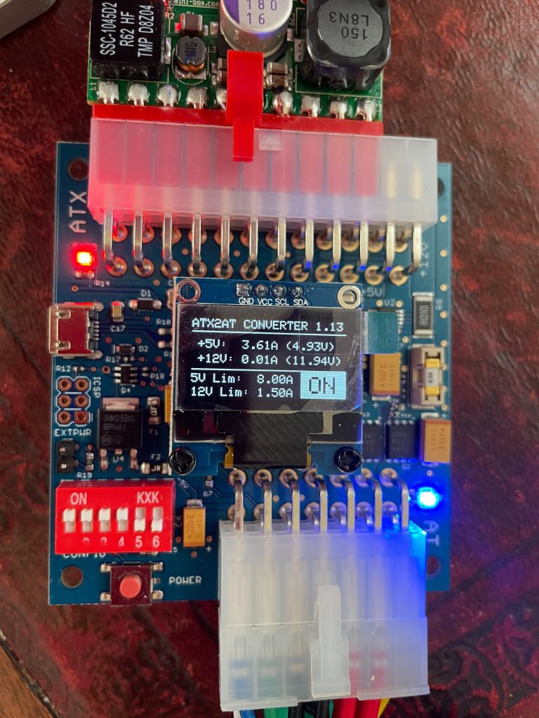
I wouldn’t probably run it for extended period of time, but it was a successful experiment showing that all those extra pins on the PODP are only optional.
This is insane. I love it! More coming?
Amazing! good job
My first computer had a pentium cpu. And we had 386s in our school computer lab. I feel old now.
This is a really cool experiment, made me feel very nostalgic
[…] But how about hacking a Pentium in? […]
This is cool! but I wonder, it almost like it was intentionally designed to be socket compatible ?
[…] But how about hacking a Pentium in? […]
dude this isn’t computer science. This is black magic!
Go talk to a priest man!
Joking apart, this is FANTASTIC!
Uhm, what’s that ATX2AT you’ve got there? 🙂
I suspect a proper adapter could be made to connect more of the pins and maybe connect the WB/WT pin to a jumper and ensure stability.
Hi, Where can we buy ATX2AT device?
Not sure if you can buy one as it was a kickstarter campaign a few years back. But since it is an open-source hardware you can build your own using https://x86.fr/category/electronics/atx2at-smart-converter/