In this post, I am comparing several options from the first wave of Pentium chipsets. The subject of the test is loosely defined as Socket 4 and Socket 5 PCI chipsets from Intel and other vendors from the 1993-1995 period. Specifically the following chipsets will be compared:
- Intel 430LX (Mercury)
- Intel 430NX (Neptune)
- Intel 430FX (Triton)
- Intel 430HX (Triton II)
- Intel 430TX (Triton III)
- ALI M1451 Aladdin
- UMC UM8890
- SiS 501
- SiS 5511
- OPTi Viper-M
- VIA VT82C570MV (Apollo Master)
Testbeds
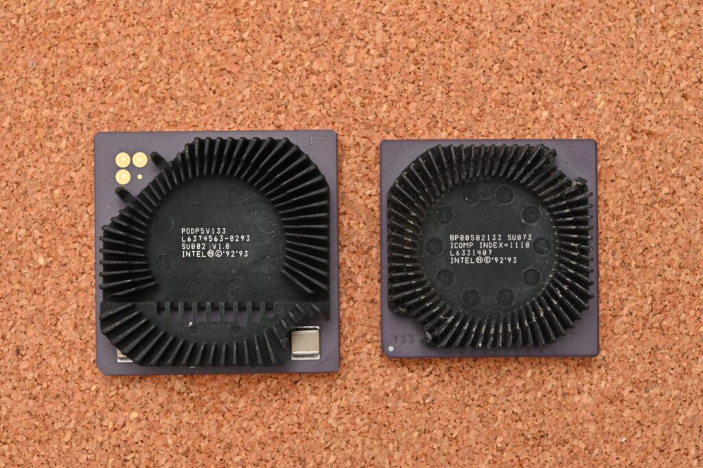
Despite comparing chipsets across different socket generations (Socket 4, 5 and 7), it is important to be using the Pentium CPU running at the same internal and bus speed. Fortunately, the ordinary Pentium 133 MHz (66 MHz Bus and 2x multiplier)can be easily matched against Pentium Overdrive 133 MHz for Socket 4 running at the same internal and bus speeds. In fact, the PODP5V133 CPU is internally a Pentium 54C, that is just adapted to run on a 5V motherboard which makes it a perfect choice for the test.
Motherboards
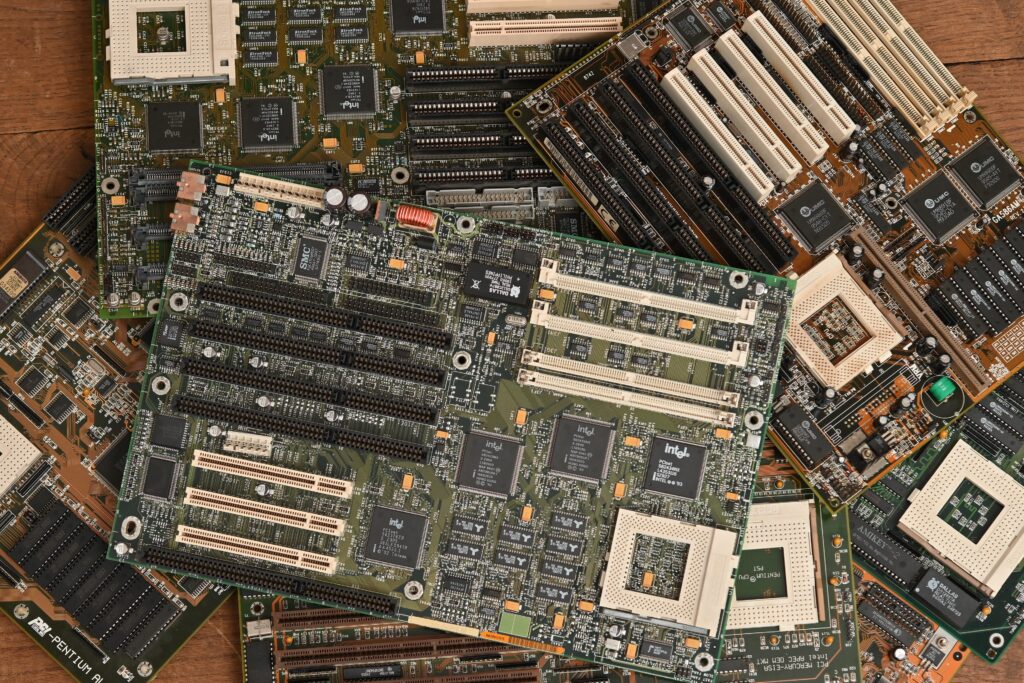
Several motherboards featuring a particular chipset were evaluated. I tried to pick the best one I could find. I ended up using the following boards:
- Intel Premiere/PCI board (Batman’s Revenge) with Intel 430LX chipset (Socket 4)
- Intel Premiere/PCI II (Plato) with Intel 430NX chipset. I modified this board to support 2x multiplier. (Socket 5)
- Intel Advanced/EV (Endeavor) with Intel 430FX chipset (Socket 7)
- Gigabyte GA-586HX with 430HX chipset (Socket 7)
- Superpower Computer SP-586TB with 430TX chipset (Socket 7)
- Gigabyte GA-586AM with UMC8891BF chipset (Socket 5)
- Microstar MS-5107 with ALI M1451 chipset (Socket 4)
- Gigabyte GA-586AP with ALI M1451 chipset (Socket 5)
- Elitegroup SI5PI AIO with SiS 501 chipset. This motherboard has been modified to support 2M cache. (Socket 4)
- Abit PG5 with SiS 5511 chipset (Socket 7)
- FIC PA-2000 with Via Apollo VT82C570MV chipset (Socket 5)
Some of these boards (notoriously all Intel motherboards) have only limited BIOS tweaking options. In absence of direct BIOS settings I used hidden settings, BIOS modifications and chipset register programming to ensure that all performance-critical options are enabled so that the chipset performs at its best.
Others
- Diamond Stealth 64 PCI VGA card with 2MB DRAM and S3 Trio64V+ chip
- 16MB EDO ram 50ns. Configured as either FPM or EDO (where supported).
- Adaptec AHA-2940U PCI SCSI controller with 512MB + 1GB disks emulated using SD2SCSI v6 device
- MS-DOS 6 and Windows 3.11. MS-DOS running in real mode.
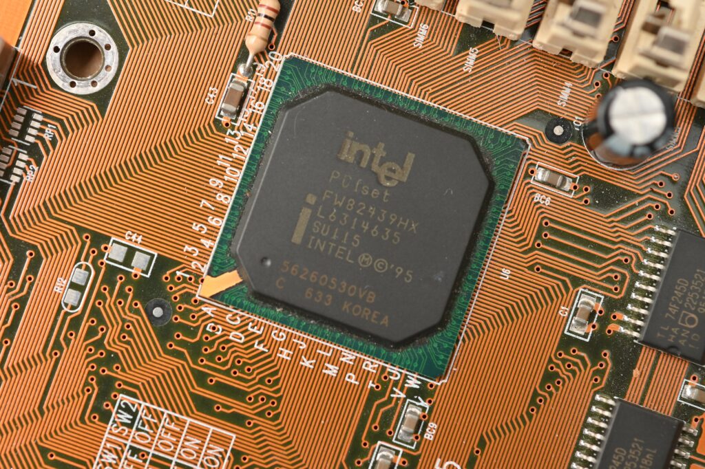
Intel 430LX Mercury
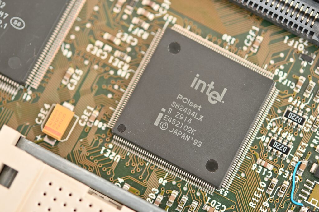
The 430LX is the original Pentium Socket 4 chipset from Intel launched alongside with Pentium 60/66 CPUs. It is a 4-chip design with one system controller (82434LX), two LBX accelerators (82433NX) and a PCI/ISA SIO bridge (82378ZB). Optionally, in an EISA configuration there could be 82375EB + 82374EB chips raising the total number of chips to five. And that’s without any I/O or IDE controller which often was a discreet infamous CMD640 or RZ1000.
The chipset can be configured with either 256kB or 512kB of either asynchronous or rarely synchronous burst SRAM modules. The cache is often soldered on the motherboard with no option to upgrade. Unlike other chipsets doesn’t need the external tag and alter chip which is integrated into the chipset. The memory controller can handle up to 192M of RAM thanks to its 6 RAS lines. Memory timing is relatively slow at (7/11/14)-4444. EDO modules can be used, but EDO timings are not supported. On the other hand, all of the supported memory can be cached.
Performance-wise the chipset delivers average performance. It is obviously beaten by all Intel successors, but performs favourably against 3rd party options, especially considering it only has 256k of L2 cache.
Intel 430NX Neptune
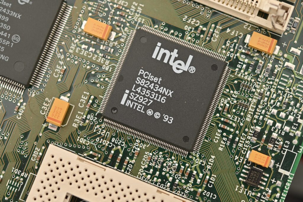
The 430NX Neptune is scaled up 3.3V version of the Mercury chipset. Together with Pentium 90 CPU, it was launched in March 1994. The feature set is similar to Mercury. Nevertheless, the chipset also has some significant improvements. With the help of the integrated APIC in the P54C CPU, it supports multiple CPU configurations. It has two more extra RAS lines which together with 16M chip support improves installable memory size up to 512M of fully cached RAM. It officially supports 50 MHz bus speeds (used by Pentium 75 chip) with optimised refresh and timings. The cache interface is identical, however, the memory controller has one clock decreased lead-off latency improving memory cycle to (6/10/12)-4-4-4.
In benchmarks the chipset shows up to 15% higher RAM throughput which translates to approx. 3-4% higher performance compared to 430LX.
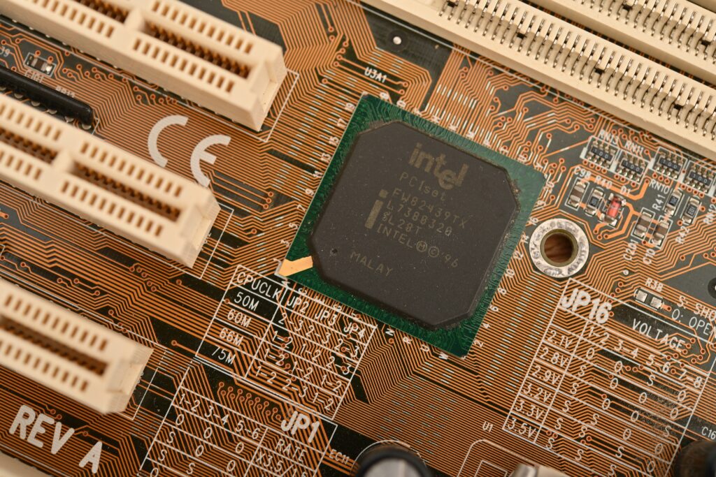
Intel 430FX Triton

The popular 430FX Triton is a member of next-generation Socket 5 chipsets designed exclusively for 3.3V P54C chips. It was the first truly mainstream chipset that appeared on many different motherboards and sold in large quantities. Compared to the 430NX Neptune chipset it succeeded, it has many new features and performance enhancements. It supports the new pipelined-burst L2 cache configuration with noticeably reduced L2 latencies. This configuration is much more common than the synchronous burst cache variant found on some earlier chipsets and both provide substantial gains over traditional asynchronous L2. It was common for the cache to come installed on dedicated COAST (Cache On A Stick) slot allowing for easier upgrades. On the other, there were also some low-end cache-less motherboards or motherboard with traditional asynchronous SRAMs. I’ve done a comparison of different 430FX cache options in this post.
The memory interface is also much more refined. EDO rams are now supported which significantly improved read timings to (7,9,12)-2-2-2. The latency when using standard FPM improved too.
On the other hand, there were also some compromises. The 430FX was designed for mainstream computers. Compared to the Neptune the chipset no longer supports multiple CPUs. The number of RAS lines went down to 5 which reduced the maximum RAM size to 128M. 430FX motherboards have 4 SIMM slots only. The first RAS line is reserved for on-motherboard RAM which some had. The full tag space is no longer integrated into the chipset and the cacheable limit is only 64MB. These look like big losses, but 64/128M was still aplenty in 1995.
Even more significant changes can be seen in the south-bridge where the 82371FB (PIIX) chip introduced bus-master DMA support which was clear step up from previous buggy CMD640 based designs.
Performance of this chipset is top-notch second only to the 430HX. Both in low-level memory tests, PCI transfer speed and application it consistently beats the competition. However, if the Triton chipset is configured with asynchronous cache it doesn’t perform nearly as well and the performance drops to average numbers. It is not without surprise that due high latency of writes, asynchronous SRAM configs can be beaten even by cache-less configurations. Clearly, the Triton was designed to work with a pipelined-burst cache in the first place.
Intel 430HX Triton II
The high-end successor of Triton technically belongs to the Socket 7 era. But I thought it is a good idea to have it included as a reference. The 430HX is a significantly refined Triton designed for high-end use in servers and workstation. It came in a new BGA package. The chip count was reduced from 4 to 2 bringing back the traditional north/southbridge design. Multiple CPU support is back. On the other hand, the chipset finally dropped the support for asynchronous and synchronous SRAMs. Pipelined-burst SRAM is the only L2 option.
As for the RAM controller, 8 RAS lines are back improving the maximum RAM size to 512M. Depending on the configuration of the tag SRAM the cacheable limit is either 64M or 512M. Both EDO and FPM configurations have reduced latencies and all sorts of buffers are deeper.
The chipset officially supports PCI 2.1 specification namely PCI. Even more, changes are in the south-bridge (PIIX3) controller where we see the first-ever implementation of USB.
The 430HX showed a great performance in this competition. However, despite reduced timelines and deeper buffers, the lead over 430FX isn’t that big. The same can be said about a gap against 430TX. Most likely a faster CPU than P133 is needed to see its full potential.
Intel 430TX Triton III
One could argue that the Triton III doesn’t belong to this test. Intel’s last Socket 7 chipset is more modern than any other chipset in this test. But I thought it is a great idea to include it anyway.
It has several improvements over the previous Triton chipset. It is commonly paired with 512kB of pipelined-burst cache which is also the maximum it can handle. Apart from FPM and EDO it also supports SDRAM modules with up to 6-1-1-1 timing.
On the other hand, 430TX being a mainstream-oriented chipset had some feature reductions compared to the high-end HX. The chipset does not support multiple processors and features like parity/ECC RAMs. Only 64M of RAM can be cached which was hardly an issue back in 1996 when it was released.
The chipset obviously won most of the individual benchmarks, however, the difference compared to 430FX/HX is small. SDRAM interface doesn’t seem to bring any substantial gains over EDO technology.
SiS 501
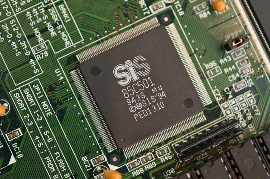
The first non-Intel chipset in my comparison is a solution from SiS. Released in 1994 it is a competitor of the 430LX chipset. It supports both P5 as well as 3.3V P54C CPUs. Three chip design consists of 85C501 system controller, 85C502 Local Data Buffer (the equivalent of Intel’s LBX chips) and 85C503 System I/O chip.
The chipset offers flexible L2 cache configurations from 64k to 2048k. The L2 is typically realised using asynchronous chips, optionally configured in a dual-banked mode requiring not less than 18 SRAM chips. A much less common configuration uses synchronous burst SRAM chips which allow achieving tighter cycles. Depending on the cache size up to 128M of RAM is cacheable.
The memory controller only has 4 RAS lines, however, 16M chips are supported so that the chip can support up to 128MB of RAM. The read latency is the same as on the 430LX, write latency is somewhat improved. EDO timing is not supported (but EDO RAMs can still be used in FPM mode).
The performance of this chipset is mediocre. In stock 256k L2 configuration, it finished my tests as the second last. Half-way between the worst ALI M1451 and Intel Mercury. The results are due to relatively slow L2 timing higher than 4-2-2-2 with 15ns SRAM chips.
However, the support 2MB of L2 cache configuration can make the chipset competitive when upgraded.
SiS 5511
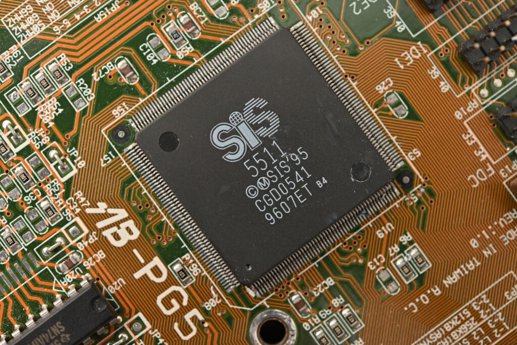
The SiS 5511, or better said a combination of SiS 5511 5512 and 5513 chips is the successor of the original SiS 501. It has many improvements over its predecessor. It does support up to 512MB of RAM with up to 256MB can be fully cached. Apart from asynchronous cache it supports pipelined burst SRAMs. DRAM interface has been also modernised. It supports EDO RAM. Quite unique feature is support of interleaved RAM banks which improves performance if all memory banks are populated with matching modules. However, this feature is only available with FPM RAM.
When using EDO RAM and pipelined-bust cache the chipset delivers solid performance. Not a Triton-level performance but matching UM8891BF chipset. Well ahead of SiS501 and other 1st gen Pentium chipset.
ALI Aladdin M1451
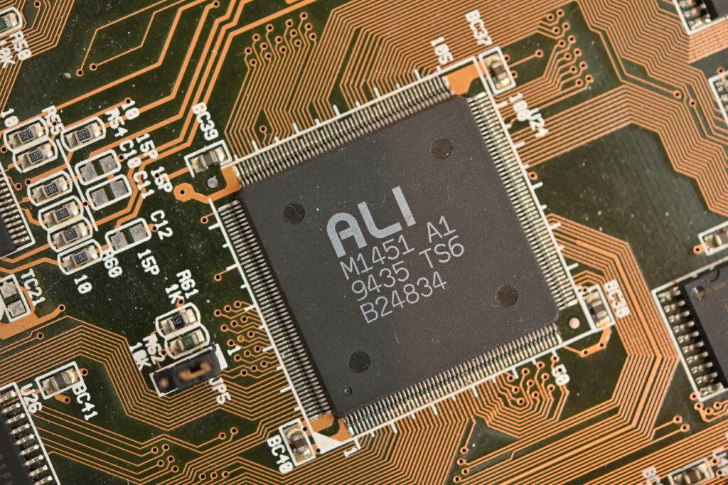
Another 430LX competitor from ALI supports 5V P5 Pentiums (although I’ve seen it adapted for P54C chips). Unfortunately, no datasheet could be found so one has to guess its specification from features on a very few motherboards that used this chipset. M1451 is budget two-chip design with M1451 north-bridge and M1449 south-bridge.
The chipset supports 256k – 1024k of asynchronous L2 cache.
The 6 RAS lines supports up to 196MB when 16M chips are used. EDO timings is not supported.
Except for a decent memory write performance, this chipset showed the slowest overall performance with particularly bad RAM read speed. That caused it to be the loser of this competition. However, the application performance, especially Quake, can be greatly improved by upgrading L2 cache to 1MB. When doing it the performance can match 430LX chipset with 256kB.
OPTi Viper-M
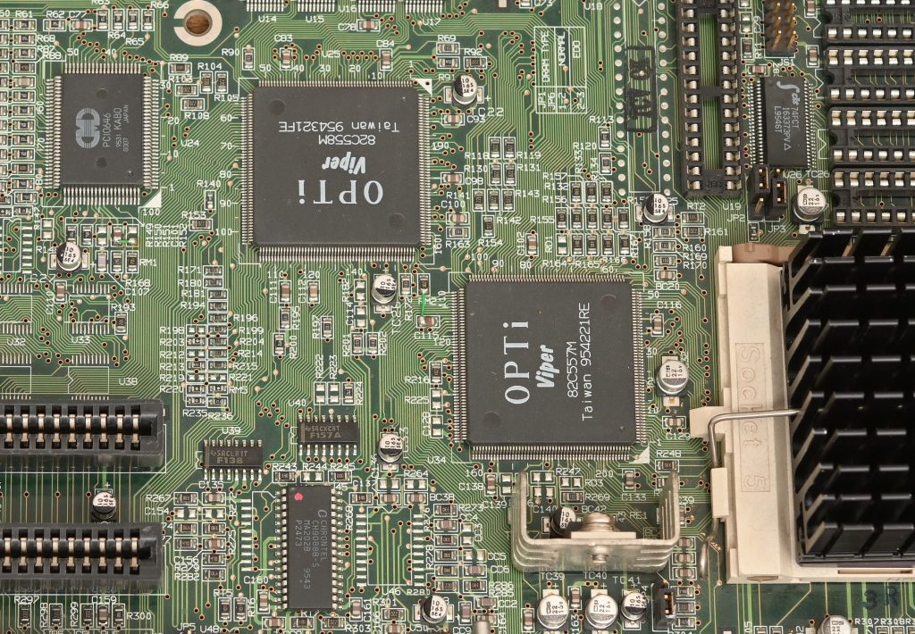
Viper-M is a Pentium chipset made by well-known 386/486 era chipmaker. One of several OPTi chipsets produced in early Pentium days. The M in the name stands for Multimedia which was a buzzword of the day. On paper the chipset is a very capable proposition, matching or exceeding Triton feature set. Supports both asynchronous as well as pipelined burst cache thanks to the standard COAST modules. Integrated IDE with bus master support. A bit unusual is support for both PCI as well as VL-Bus slave ports. Although the VL-Bus is not a true local bus as on 486 but a feature of the host bridge.
One interesting feature of the Viper-M chipset is that next to usual write-through and write-back also supports a unique adaptive write-back mode where a write-back cycle is converted to write-through depending on the state of the memory interface which might be beneficial in certain situations.
The Viper-M proved to be the most problematic chipset in the group. I got it on an Acer branded motherboard with only very limited tweaking options available. It showed compatibility issues with popular apps using the popular DOS4GW extender. It was necessary to replace it in order to run benchmarks.
Performance is a bit lagging though. Relatively slow write performance resulted in weak Quake score. One interesting fact is that at least on the motherboard tested there was no difference when used with pipelined-burst or asynchronous cache. The performance was identical. Clearly the pipelined burst cache did not enjoy the benefit of improved cycles.
UMC UM82C890
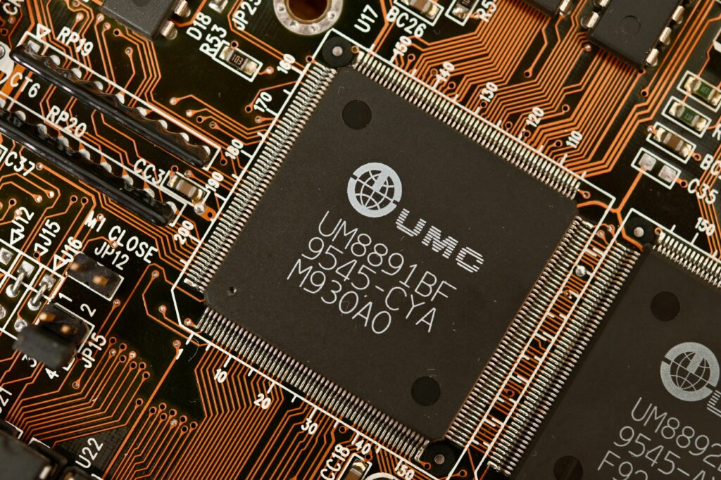
A popular 386/486 chipset maker – UMC also produced a limited number of chipsets for Pentium. I was keen to test this one as there are some claims that this is actually a crude modification of 486 chipsets delivering abysmal performance. Upon reviewing the performance of the UM8891BF variant of the chipset, I can confirm this is not the case, at least for the board and revision of the chipset I tested.
The UM8890 consists of UM8891BF/UM8892BF memory controller and UM8886 PCI/ISA bridge and IDE controller, which is more or less equivalent to the Intel Triton chipset with a similar feature set. There is also an AF revision of the UM8891, which doesn’t support pipelined-burst cache or EDO, but I did not have one for tests.
It supports asynchronous as well as pipelined burst cache up to 1024k. It has 4 RAS lines supporting up to 128MB of RAM, which can be either FPM or EDO with x-2-2-2 timings.
Given my test motherboard (GA-586AM) has both a COAST slot as well as DIP sockets for asynchronous SRAMs, I was able to test the chipset in several configurations. First with pipelined-burst 256kB cache and then with asynchronous cache configured to 256k, 512k, and 1024k. The pipelined burst was clearly the fastest, with the 1024k configuration getting close to it in application tests.
VIA Apollo Master 570 (Plus version)
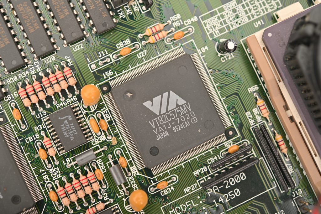
A traditional chipset maker -VIA Technologies was relatively late in the game with their first Pentium Chipset – Apollo Master. The chipset launched in 1995 had support for both 3.3V P54C as well as 5V, but I am yet to see it in the Socket 4 configuration.
The VT82C570MV is a 4 chip design with VT82C575MV system controller, VT82C576MV PCI controller and two VT82C577MV data-buffers. Often it is also paired with the fifth VT82C416 that handles CMOS storage and keyboard/PS2 controller functionality.
The unique “feature” of the Plus version (marked by -V suffix) over the original version is that it doesn’t have support for the pipelined-burst cache. But it does support traditional asynchronous or non-pipelined burst configuration up to 2MB (in dual-bank configuration). Thanks to up to 10bit tag all installed RAM is fully cacheable.
The RAM controller supports FPM, EDO and burst-EDO RAM modules that can be mixed up to 512M max capacity in the maximum configuration.
A unique feature of this chipset is that it can be used with only one 72pin SIMM module. Almost all other Pentium chipsets need two SIMMS to fill the 64bit bus. However, unsurprisingly this leads to even worse performance.
Sadly I couldn’t test the chipset in its best configuration with pipelined-burst and also my board had problems running with full stability in 3-2-2-2 mode thus the cycle had to be reduced to 4-2-2-2. That surely helped to last or almost last in most tests. Not even above average RAM read speed, thanks to using EDO RAM saved it from a poor showing in application tests. Likely the problem is in slow write speeds.
Test results
First let’s have a look at L2 cache and memory read/write speeds as measured by speedsys tool
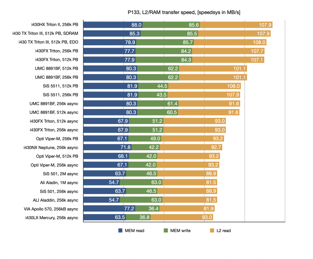
As you can see Tritons are well in lead followed by the UMC chipset where the difference between PB and the async option is smaller than one might think. Intel chipsets score particularly well in write speeds and that might be the secret sauce of why they are so well ahead in application tests. The rest of the group shows comparable performance with some minor differences in individual numbers.
Next is my favourite test. The framerates in Quake 1.06 timedemo at 320×200.
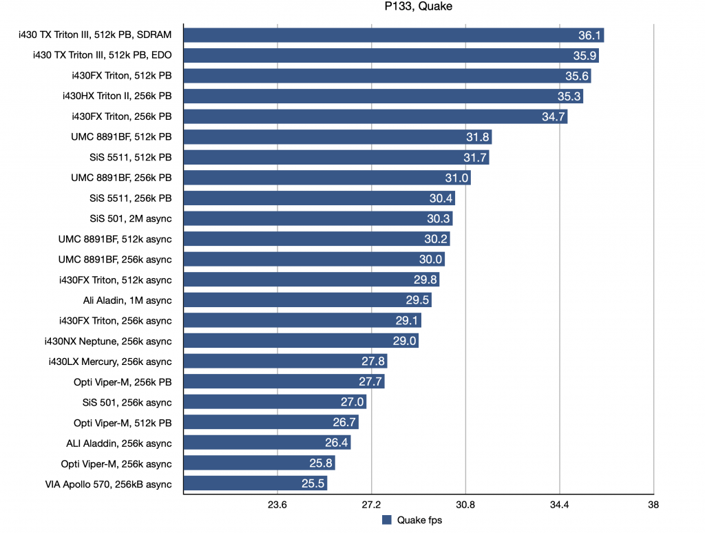
Triton chipsets are still leading the pack followed by the UMC and SiS 5511. The Opti Viper and especially VIA Apollo both show quite poor performance in default config. The VIA is the slowest in all configurations. It is more than 40% slower than the winner. However, Quake is a test where the slower RAM speed can be somewhat compensated by having a large L2 cache (so that the slow RAM is accessed less often). Upgrading L2 cache size nicely improved the performance of SiS and Aladdin chipsets and made them competitive again.
Winstone 95 is a nice Windows 3.1 based benchmarks that should indicate performance in real-world business-oriented productivity apps of the era. Like Microsoft Word, Excel, Wordperfect, Paradox and others.
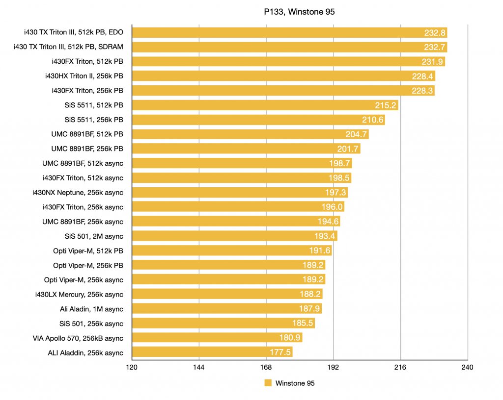
The rankings are unchanged here. Triton chipsets dominate everyone else. ALI Aladdin, VIA Apollo and SiS 501 are lagging well behind. Again their performance can be improved by upgrading L2 cache size, although the effect is smaller than in Quake.
Test results
This story is open ended as I intend to continue in my research. Specifically I’d like to do the following:
- Add more chipsets. Such those from OPTi (Python, Cobra), VLSI, VIA, UM8890 revision AF and possibly more
- Source better SRAM chips or motherboards sporting SiS501 and ALI Aladdin that would allow more aggressive L2 timings
As you can see the choice of chipset can make a significant difference. The gap between the first and last chipset in the Quake test is 38%. Which is equivalent to two CPU classes.
The results clearly show that Intel Triton (any generation) is the undisputed king of this generation of chipsets. It just shows how big deal the introduction of this first-party chipset was for the Pentium CPU.
The fourth place is shared between SiS 5511 and UMC8891 chipsets. The results of the latter came as a surprise after reports about its horrendous performance and outdated 486 design. Perhaps I was just lucky in the chip revision lottery?
The original Mercury and Neptune chipsets delivered a solid performance which was adequate when they came to the market. For a long time, they were etalons everybody wanted and compared with. The small improvements in 430NX proved to be useful for it to beat the 430LX.
And finally SiS 501 and Aladdin. Those chipsets are lagging behind the Intel offerings they tried to compete with. Back in the days, they provided high value given by their price and level of integration. However, nowadays the support of 1024k and 2048k L2 cache gives them tuning potential if you can find the required SRAM chips. The SiS 501 is the better of these two if you have to choose.
A fantastic comparison – thanks!
I didn’t know that there was a UMC based chipset for the old Pentiums… that would be nice to have.
I remember the 430LX from back in 95 – I was not aware of the lame timings but many years later on, when tinkering with end era, but nonetheless “archaic”, 486 boards, I was shocked that the old P5 chipset seemed unnecessarily neutered in comparison.
Is there a way to tune up the old 430LX based boards?
Take care,
viktor
I love this old history stuff. As it happens, I mostly sat out the Pentium era. I started with a 486DX laptop running MS-DOS and a very fast disk accelerator in my many otherwise-useless MB of extra RAM. Think I had 8 MB after an upgrade. I was never a fan of Windows 3.1 because I hated overlapping windows on small monitors and I mostly thought the main function of Windows 95 was to reboot itself. When it finally arrived, I jumped straight to Windows NT 3.51 (soon 4.0) on a Pentium Pro system. Finally a real 32-bit OS you didn’t need to reboot every time you blinked the wrong way. The funny thing was, people who were invested in 95/98 never got the news about just how much better/faster/stronger Windows NT on a Pentium Pro was compared to Windows 98 on a regular Pentium. Outside of the workgroup server space, the Pentium Pro was often described by the press (for the benefit of the unwashed masses) as a disappointment. The actual reality of the Pentium Pro is that it immediately thinned out the competitive RISC space, because the PPro was delivering the kind of performance they had assumed the sucky x86 architecture could never, ever, under no circumstance ultimately deliver. Only it turned out that the memory subsystem was actually worth far more than the core architecture, and by this point the PPro had a deeply out-of-order core coupled to a proper split transaction bus and insane amounts of L3 cache memory (in a very expensive multi-chip module bonding exercise, but the results spoke for themselves). The problem was that the PPro’s ability to run the the 16/32 instruction mix of Windows 95/98 was rather poor as first released. (This was tweaked in later variants.) However, on pure 32-bit code, it ran like a bat out of hell, relative to the era. Unlike some of the RISC competitors, the deep OOO core made the PPro rather insensitive to heavy/heterogeneous workloads; it just kept rocking on. Other “cleaner” machines tended to benchmark better than they multi-tasked when heavily loaded. For my money, the PPro was the most revolutionary product Intel ever introduced. They gained instant credibility in the workstation/medium server space with 4-way SMP. The awesome Core2Duo—we didn’t now about Spectre yet—was the next biggest bump in Intel’s history, and this was basically a reprise of the original PPro, via Tualatin, if memory serves. I think it’s a story worth telling if your series wants to cover a few more years in the aftermath of the Pentium glory days.
The PPro was awesome but very few people had one… and even rarer was a system featuring the 1MB version.
I vividly remember the “gaming Press” tearing the PPro a new one, when it feautured outstanding performance in software that mattered – a PPro + Voodoo was The Quake machine.
Awesome test! Don’t forget the VIA chipsets! From vp1 to mvp4 (though some of the latest are more like ss7). Still, I remember when they arrived to the market they were labelled “intel killers” not much because of the performance, but because of the features. Specially from vpX/vp2 and on.
Thanks. VIA motherboards tend to come on newer Super Socket 7 motherboards. But I’ve seen some older Socket 5 ones. Will try to get one of those.
Nice article, i wonder, what are the motherboards used? i can recorgnize the Batman and Pluto boards, but not the others. Speaking of other chipsets, i wonder how would stack the ALi M1511/M1512/M1513, i recently found an old Fujitsu pc with the Acer V50LA motherobard which happens to use that ALi chipset
Thanks. Please scroll to the top to see the list of motheboards used.
I expect the Ali M1511 (Alladin II) to be roughly on par with second-gen non-intel chipsets in the test. Like SiS5511. Not too bad a bit below Intel offerings. But I know for sure once I get one!
i just noticied, i probably expect around that level as well, i don’t know of any other ALi M1511 boards besides the Acer V50LA V50LC and V52LA, ALi M1521 was used on the Acer V55, V55-2, V56LA and V56LT. My Acer V50LA motherboard is currently paried with 64 MB 50 ns EDO, onboard ATI mach64 CT and a Pentium 100
Great article although I’m surprised you didn’t include the 430VX chipset, the 1st chipset with SDRAM support. A sort of progenitor for the TX this is actually the Triton III chipset – the TX was called the Triton TX – it has support for both Dimms and Dimms (4xSimm slots/2xSimm slots & 1xDimm Slot/2xDimm Slots, consumer level features like TX but still the Triton II southbridge with DMA Mode 2/PIO Mode 4 IDE.
VX was a great chipset. Ran a VX board for some time that would run a PMMX 233 stable at ~266/75. With SDRAM installed and timing tweaked it was very quick. Great rig before the SS7 boards showed up.
In the mid to late 90s I went through a lot of different random motherboards I found at the local Re-PC. Mostly Socket 3 and later Socket 5/7 stuff. They were practically giving them away so I would buy a board, take it home, play with it for a while and move on. A few great ones became my main PCs for some time.
One of the worst I still remember was a P60 VLB-based board – I (much later) found out it was an AMI Excalibur with an OPTi 597 set – I think one of their last before they exited the market. I didn’t know what it was when I saw it in the store, but I had never seen or heard of a VLB Pentium board, so I bought it. I was pleasantly surprised to see that it easily ran stable at 66MHz, and there was only one switch to be flipped to make it happen. I could only get it to run with a maximum of 16MB RAM. It didn’t even have a ZIF socket for the CPU. It had the awful looking puke colored AMI BIOS that looked like it jumped right out of the 386 era. It seemed like this was a prototype board that somehow went into production.
Unfortunately even with a decent VLB graphics card installed it was dog slow at most DOS games. At the time I had a 5×86 running at 160, and even in my favorite Pentium optimized FPU intensive games like Quake or Terminal Velocity, the 5×86 made the P66 look like a joke.
I’ve read some comments online stating that the OPTi VLB chipsets did some tricks with VLB to make it work with the Pentium, since VLB was basically an extension of the 486’s external bus that didn’t translate in any way to the P5. Don’t know how true this is, but it would make sense. I’m sure bridging the VL bus through the chipset negated almost all of the features that gave VLB its performance edge over early PCI.
It eventually got banished to cable modem router duty running FreeBSD with a few 3c509 cards installed into it. Fortunately for that role it was perfect and chugged away for probably a few years without a problem.
I really wish I still had that thing so I could do some benchmarks to see how pathetically slow it really was. In all of my PC tinkering days of my youth in the 90s, that was the only P66 I ever saw, and probably the worst example of it too.
The VIA VT82C570M Apollo master was an interesting P54C socket 5 chipset as well from 1995.
− VT82C575M system controller
− VT82C576M PCI bus controller
− PCI-2.1 compliant
Burst Synchronous (Pipelined or non-pipelined), asynchronous SRAM and Cache Module
support
cache support for: 0K/128K/256K/512K/1M/2MB
Memory support: FPM/EDO/Burst-EDO-DRAM
8 banks up to 512MB
I have a FIC made one? from a unisys CWD-5001, the actual socket they used on it states it’s socket 7 however. officially the board only has listed jumper and divider settings from 75mhz up to 166mhz. But playing around with them there’s an unlisted one that will allow the 200mhz pentium to work. No MMX support as the chipset pdf states only voltages supported are 5v and 3.3v.
The FIC board lists these however as the only voltage options.
3.384v (CPU STD OR VR)
3.54v (CPU VRE)
Thanks. A VIA chipset on FIC motherboard similar to yours has been added to the test. Not the best performer as it turns out.
Hello,
I discovered your articles through the ultimate hardware section on win3x.org.
I have this board: https://www.win3x.org/uh19/motherboards/5000
It looks like you provided the image.
It had severe battery corrosion damage and while I doubt it will ever run again, I would like to use it as repair/soldering practice. If you still have the board and have the time, I would greatly benefit from some high res pictures from around the battery area. I’m leaving my email if you’re able to reach out.
Thanks for reading, and if nothing else I’m glad I discovered your articles.